Проведено исследование основных причин возникновения фотодиодов с токами утечки в МФПУ на основе антимонида индия. На большом объеме МФЧЭ установлена связь одноточечной дефектности с напряжением пробоя, диффузионной длиной, концентрацией основных носителей и плотностью дислокаций. Представлены характерные распределения дефектности по пластинам антимонида индия. Показано влияние на дефектность качества обработки пластин после резки слитков и погрешностей технологии изготовления.
In paper the causes of photodiodes defectiveness of a large format InSb focal plane arrays consisting, basically, from current leakages have been investigated. Currently achieved level of InSb FPA 320256 defectiveness is about 0.1—0.3 %, mainly due to the semiconductor material and its processing.
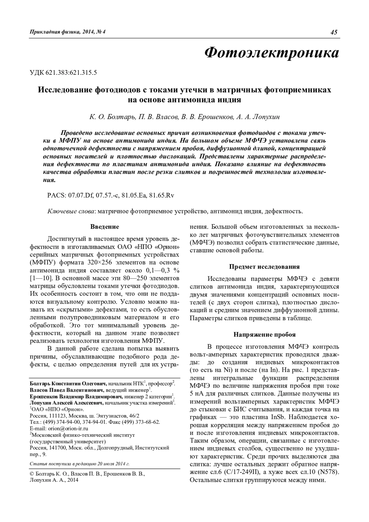
Large volume of produced FPA has allowed collecting statistical data which formed the basis of this paper in which frameworks parameters of matrix photodiodes (MPD) from InSb nine ingots are investigated.
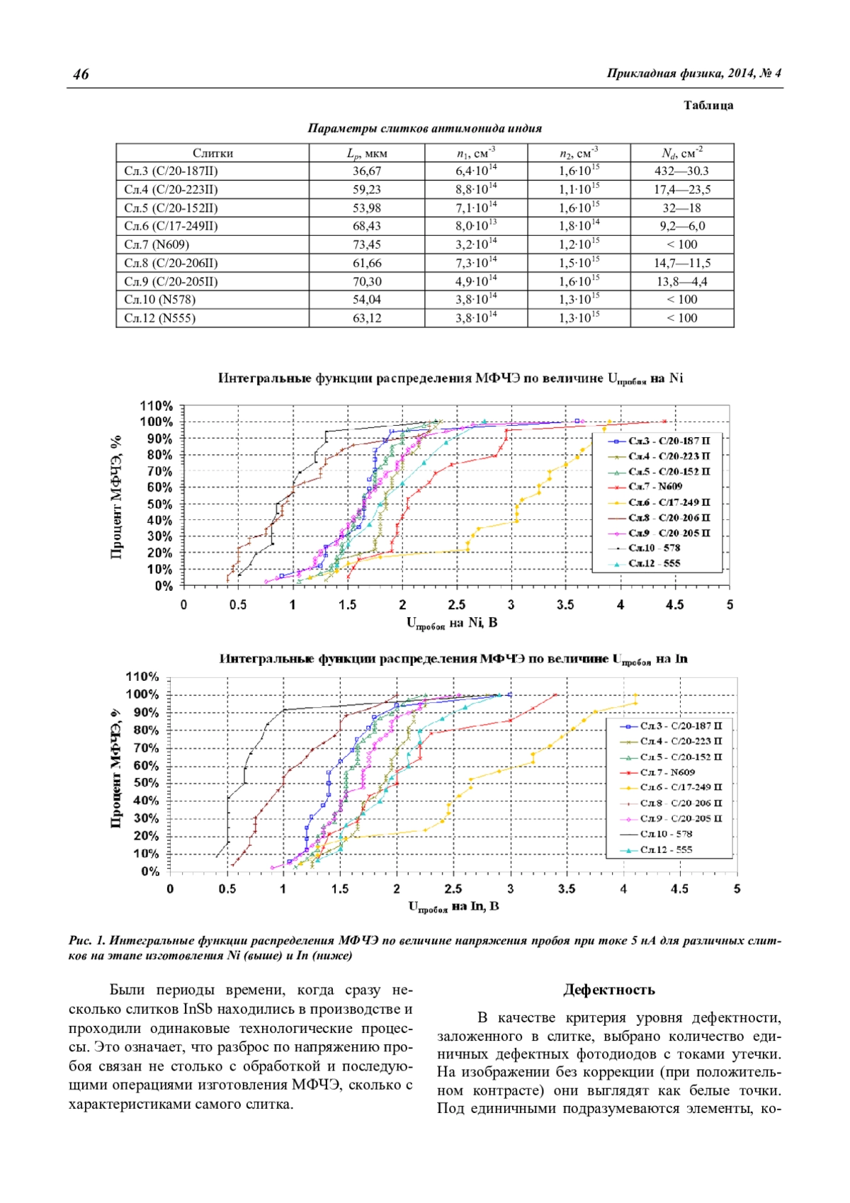
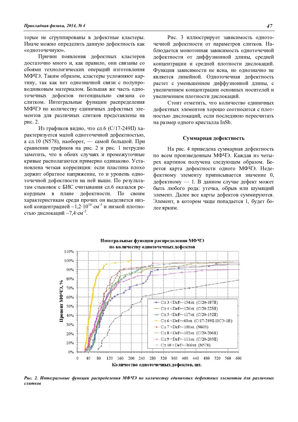
Correlation founded: if the wafer not holds back voltage, also defectiveness on it above. The ingot with low concentration of ~1014 sm-3 and dislocations low density has appeared with the minimum average defectiveness by results of bonding with a ROIC. MPD produced of one ingot and from the adjacent wafers have shown a large difference in defectiveness that it is logical to explain influence of wafers processing after is sawing.
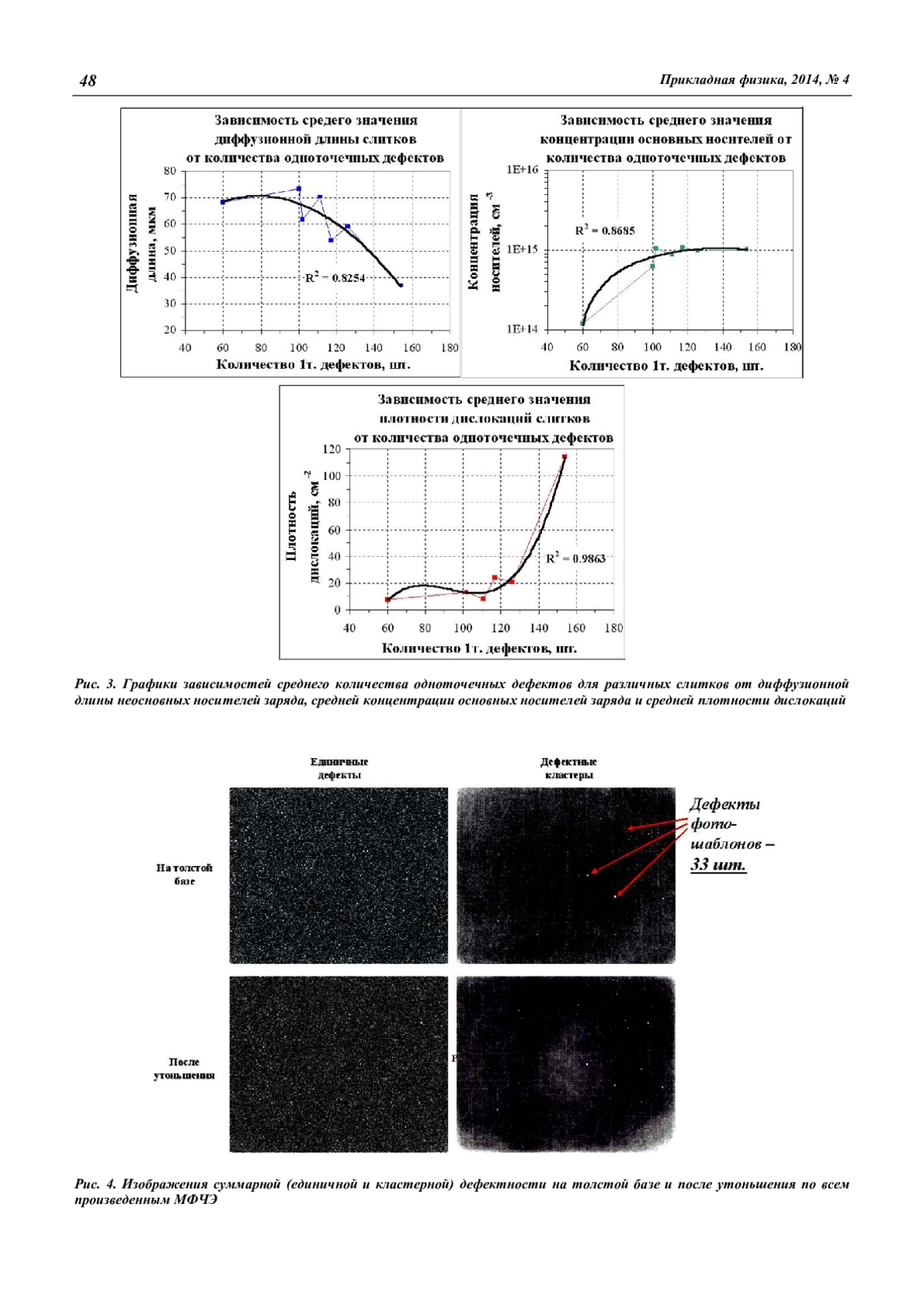
The images obtained by summing the individual defects only on thick base and after thinning have shown sufficient uniform distribution over the area that indicating a lack of process thinning influence on defectiveness. The images obtained by summing defective clusters (that is all defects, except individual) have shown allocation of corners that is connected with edge effects: unbonding and an overclamping indium bumps after bonding in corners, cracks along the edges after thinning, etc.
Thus, the main causes of leakage currents from the photodiodes had appeared:
- Dislocation density of initial InSb ingots;
- The quality of wafers processing after is sawing ingots;
- Errors of MPD producing technology (usually formed defects clusters).
Предпросмотр статьи
Идентификаторы и классификаторы
- SCI
- Физика
- eLIBRARY ID
- 22273866
Если у вас возникли вопросы или появились предложения по содержанию статьи, пожалуйста, направляйте их в рамках данной темы.